Product Jan. 22, 2019
Hioki Launches Flying Probe Tester FA1817
Test Tool Delivers Reliable Detection of Latent Defects on High-Density Printed Wiring Boards
January 21, 2019 - Nagano, Japan
The FA1817’s features and capabilities make it ideal for use in
inspecting high-density printed wiring boards. With support for a broad
range of test types, from low-resistance measurement to
high-insulation-resistance measurement, the system reliably detects the
latent defects that trouble end-users.
*1 A printed wiring board (PWB) onto which no electronic components have been mounted
Development Background
Printed circuit boards (PCBs) onto which electronic components have been mounted can be found in industrial equipment, automotive devices, consumer electronics, and other products, where they play an extremely important role by providing device operation and control functionality. To ensure their electronic components function properly, bare boards must exhibit high quality and reliability.
In recent years, miniaturization of electronic devices has seen bare boards with finer-pitch, higher-density patterns, as well as large numbers of layers, with the result that latent defects are becoming more common. Recognizing the needs of customers that wish to improve the quality of such bare boards, Hioki developed the FA1817 as a system capable of detecting a variety of phenomena that can cause latent defects, including open vias, near-open defects, micro-shorts, and arc discharges.
Key Customers
· Manufacturers of printed wiring boards
Key Features
1. Support for a broad range of test types, from low-resistance measurement to high-insulation-resistance measurement
Hioki has taken advantage of its exceptional technological capabilities in the areas of low-resistance measurement and insulation resistance measurement to deliver the ability to measure low resistance as well as high insulation resistance of 100 GΩ/250 V (when using dedicated probes and measurement boards).
The FA1817’s low-resistance measurement functionality measures minuscule fluctuations in resistance values to detect open-via defects. By means of its high-insulation-resistance measurement capabilities, the system also detects insulation abnormalities and arc discharge phenomena caused by the effects of pattern shape anomalies and impurities, voids, and other defects that exist between patterns.
2. Half the impact depth
Traditionally, probes are placed in contact with the board to carry out bare board testing in a process that leaves impact marks on the board. On high-density bare boards, even small marks can have a serious effect. Impact marks from the probes of previous products were already slight, but the FA1817 uses the High-density Probe CP1072, which was developed using proprietary Hioki technology, in order to further reduce the size and depth of these marks. Impact mark depth has been halved compared to that of previous products to minimize damage to bare boards.
3. Optimized probe movement for testing that’s up to 20% faster
By taking advantage of two top arms and two bottom arms to probe target boards efficiently, the FA1817 reduces testing times by up to 20%.
4. Defect analysis with the newly developed Process Analyzer (a standard accessory)
About HIOKI
Established in 1935, HIOKI E.E. CORPORATION (TSE: 6866) has grown to become a world leader in providing consistent delivery of test and measuring instruments through advanced design, manufacturing, and sales and services. By offering over 200 main products characterized by safety and quality while meeting an expansive range of applications, we aim to contribute to the efficiency and value of our customers' work in research and development, production and electrical maintenance. HIOKI products and services are available around the world through our extensive network of subsidiaries and distributors. Information about HIOKI is available at www.hioki.com.
January 21, 2019 - Nagano, Japan
Hioki is pleased to announce the launch of the Flying Probe Tester FA1817, an automatic testing system designed to inspect printed wiring on bare boards*1.
In addition, Process Analyzer, a newly developed application that ships
standard with the FA1817, makes it easy to create statistical data based
on on test results and to analyze defects. In this way, the system can
be used not only to perform pass/fail testing, but also as an aid in
realizing process improvements.
Development Background
Printed circuit boards (PCBs) onto which electronic components have been mounted can be found in industrial equipment, automotive devices, consumer electronics, and other products, where they play an extremely important role by providing device operation and control functionality. To ensure their electronic components function properly, bare boards must exhibit high quality and reliability.
In recent years, miniaturization of electronic devices has seen bare boards with finer-pitch, higher-density patterns, as well as large numbers of layers, with the result that latent defects are becoming more common. Recognizing the needs of customers that wish to improve the quality of such bare boards, Hioki developed the FA1817 as a system capable of detecting a variety of phenomena that can cause latent defects, including open vias, near-open defects, micro-shorts, and arc discharges.
Key Customers
· Manufacturers of printed wiring boards
Key Features
1. Support for a broad range of test types, from low-resistance measurement to high-insulation-resistance measurement
Hioki has taken advantage of its exceptional technological capabilities in the areas of low-resistance measurement and insulation resistance measurement to deliver the ability to measure low resistance as well as high insulation resistance of 100 GΩ/250 V (when using dedicated probes and measurement boards).
The FA1817’s low-resistance measurement functionality measures minuscule fluctuations in resistance values to detect open-via defects. By means of its high-insulation-resistance measurement capabilities, the system also detects insulation abnormalities and arc discharge phenomena caused by the effects of pattern shape anomalies and impurities, voids, and other defects that exist between patterns.
2. Half the impact depth
Traditionally, probes are placed in contact with the board to carry out bare board testing in a process that leaves impact marks on the board. On high-density bare boards, even small marks can have a serious effect. Impact marks from the probes of previous products were already slight, but the FA1817 uses the High-density Probe CP1072, which was developed using proprietary Hioki technology, in order to further reduce the size and depth of these marks. Impact mark depth has been halved compared to that of previous products to minimize damage to bare boards.
3. Optimized probe movement for testing that’s up to 20% faster
By taking advantage of two top arms and two bottom arms to probe target boards efficiently, the FA1817 reduces testing times by up to 20%.
4. Defect analysis with the newly developed Process Analyzer (a standard accessory)
The Process Analyzer application makes it easy to load accumulated test results data in a batch and then create statistical data from it. Test step results can be visualized using such means as value changes, histograms, and distribution maps to facilitate analysis of defects. By generating information about analyzed defects that can be provided as feedback to design and manufacturing processes, the Process Analyzer helps customers improve yields in printed wiring board manufacturing.
About HIOKI
Established in 1935, HIOKI E.E. CORPORATION (TSE: 6866) has grown to become a world leader in providing consistent delivery of test and measuring instruments through advanced design, manufacturing, and sales and services. By offering over 200 main products characterized by safety and quality while meeting an expansive range of applications, we aim to contribute to the efficiency and value of our customers' work in research and development, production and electrical maintenance. HIOKI products and services are available around the world through our extensive network of subsidiaries and distributors. Information about HIOKI is available at www.hioki.com.
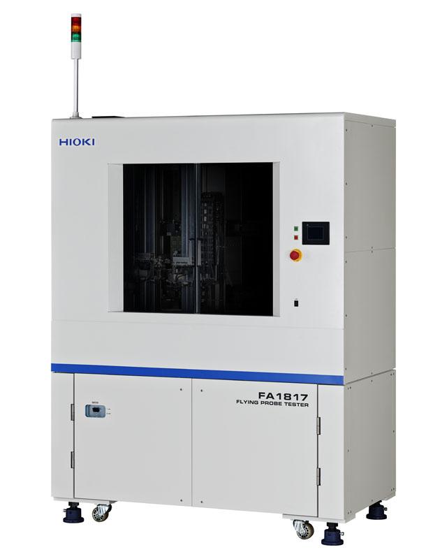 FA1817 Flying Probe Tester
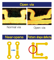 Typical board defects
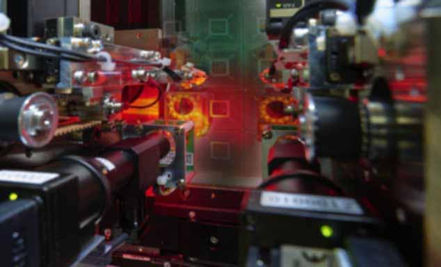 Board probing in action