Burn-in Board Testing System
This article introduces a system that can test burn-in boards used in semiconductor testing flexibly and at high speeds.
Burn-in boards are used by burn-in testers.
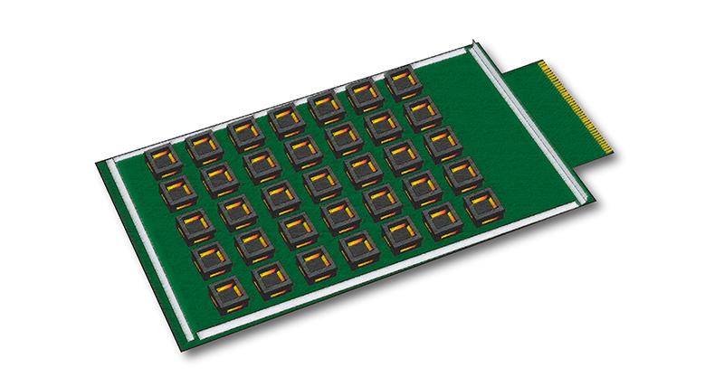
The final stage of the semiconductor manufacturing process includes burn-in testing. The goal of such testing is to discover initial defects in advance by applying temperature and voltage loads to completed semiconductors. A pedestal called a burn-in board is used to hold semiconductors during such testing.
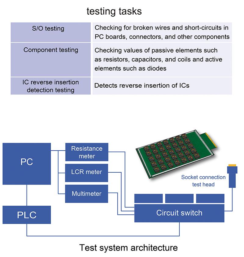
Since this board is used to apply electric signals to the semiconductors, it consists of a lattice of IC test sockets on a PCB and circuits made up of passive components such as resistors, coils, and capacitors as well as active components such as transistors and diodes. Several of these boards are loaded into a burn-in tester, which carries out the test while applying a temperature load.
Since the testing cannot be carried out properly if there is an issue with the burn-in board itself, each board must be tested.
This article introduces a reliable, high-speed test system designed to ensure the quality of burn-in boards.
Issues with burn-in board testing
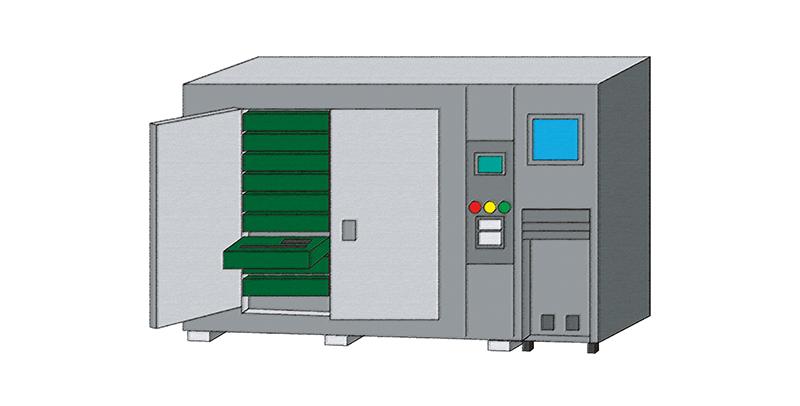
Currently, workers carry out these tests by inserting a connection test head into one IC socket at a time. Since the test heads are not fixed in place, the state of contact varies with the worker’s movements, and the testing process tends to be characterized by poor yield due to issues like needing to repeat tests a number of times.
Workers must do their utmost not to change their movements during testing. The effects of such movements, as well as the workload, increase as the test time for each IC socket lengthens. In summary, testing is characterized by the following issues:
- Poor yields and time-consuming tests
- Omitted tests and missed defects due to careless mistakes
- Variability in test results due to dependence on individual workers
- Higher workloads due to long working hours
Realizing high-speed testing and superior operability
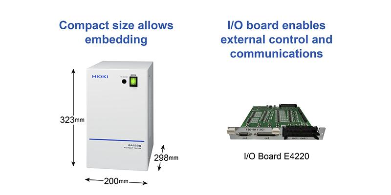
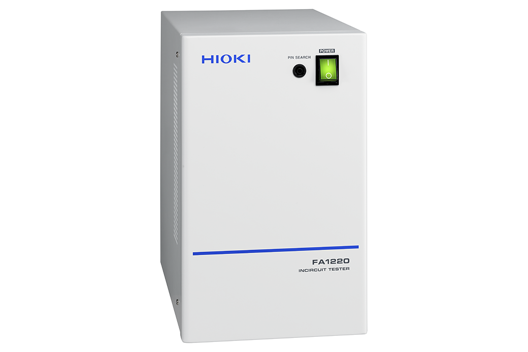
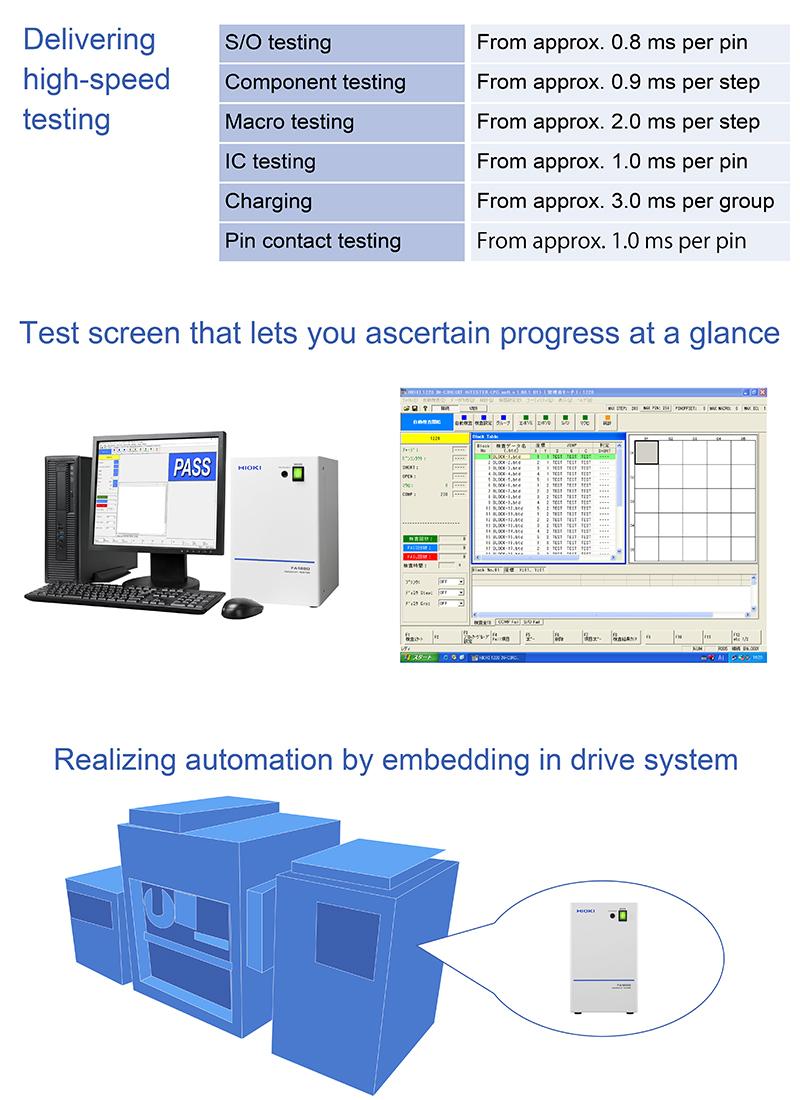
The In-Circuit Tester FA1220 incorporates a circuit switch (scanner) and measuring instrument into a compact enclosure that implements test sequences created using a computer application. An optional integrated I/O board lets the system interoperate with external drive systems, allowing it to be embedded in automated equipment.
- A foot switch makes it easy to start and stop testing and to move among blocks.
- The system can measure up to 1,024 pins.
- A test results map display (up to 32 × 32) allows untested and defective locations to be identified.
- A protective function halts subsequent testing if the self-test function identifies a problem.
- The system provides functionality for halting subsequent testing if a FAIL result is encountered.
- IC socket connection test heads currently in use can be used (requires connector fabrication).
Semiconductors are increasingly being utilized in new information technologies such as the IoT and AI.
Going forward, more and more manufacturing facilities are likely to face the need to achieve both higher quality and shorter test takt times.
The In-Circuit Tester FA1220 holds the potential to address the needs of such facilities.
Functionality and concept that make it possible to embed the FA1220 in other equipment
Despite its compact size, the In-Circuit Tester FA1220 can accommodate scanners for up to 1,024 pins.
An I/O board allows the system to be controlled from an external source, for example to start testing, and to output judgment results.
The FA1220 is equipped with functionality and specifications that are available when embedded in the customers’ systems.