Measuring the high-frequency forward resistance of PIN diodes
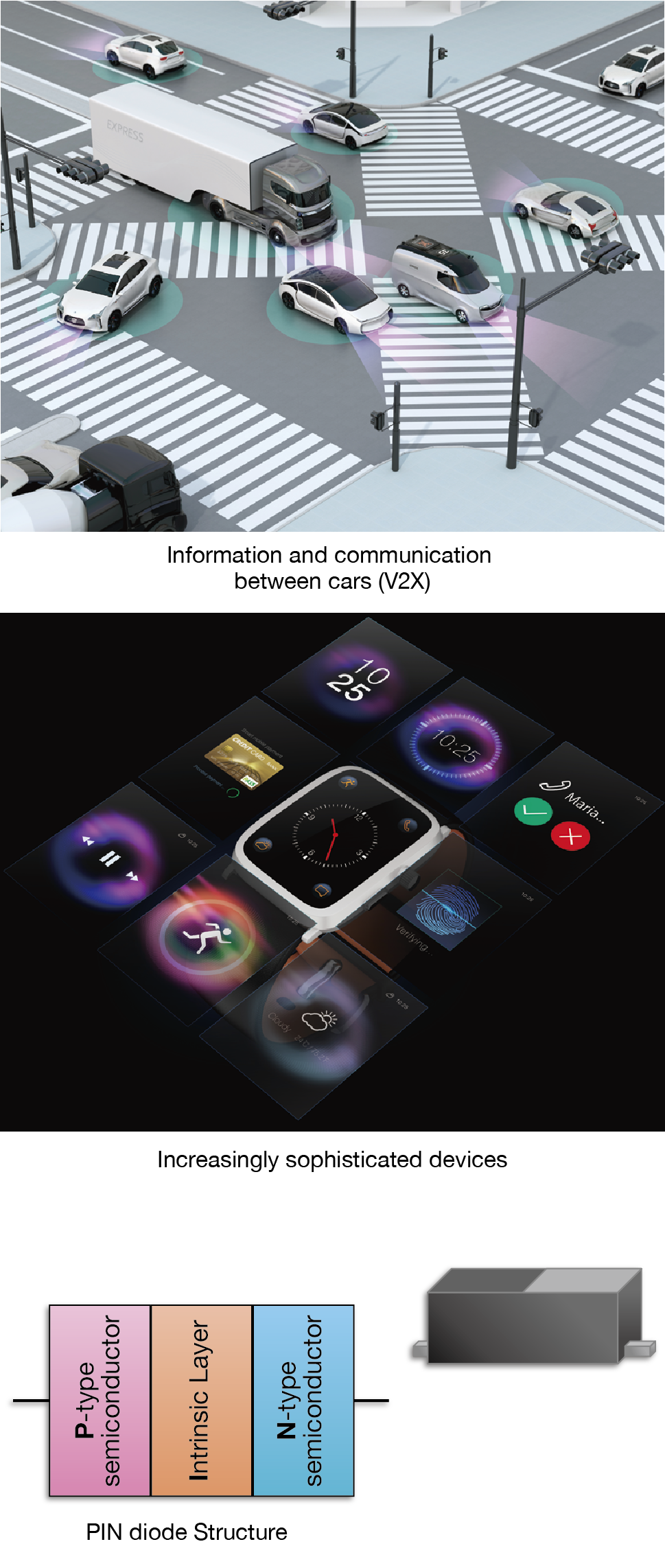
Adoption of next-generation 5G wireless technology, whose features include low-delay communications and multi-node connections, is proceeding apace. In addition, high-speed communications applications such as vehicle-to-everything (V2X), which describes communications between vehicles and other devices, are also becoming more common.
Components known as PIN diodes play an essential role in circuits that handle high-speed signals. PIN diodes are semiconductors with an intrinsic layer sandwiched between PN junctions. PIN stands for P-type semiconductor, Intrinsic layer, and N-type semiconductor.
Their characteristics include the following:
• They have extremely low capacitance between terminals in order to avoid any effect on the propagation of high-speed signals.
• They operate as a variable resistor when a forward voltage is applied to cause a forward current to flow.
As a result of these characteristics, PIN diodes are well suited to use in auto gain control (AGC) circuits, transmit-receive switching of high-speed signals, and switching operation.
How to Test
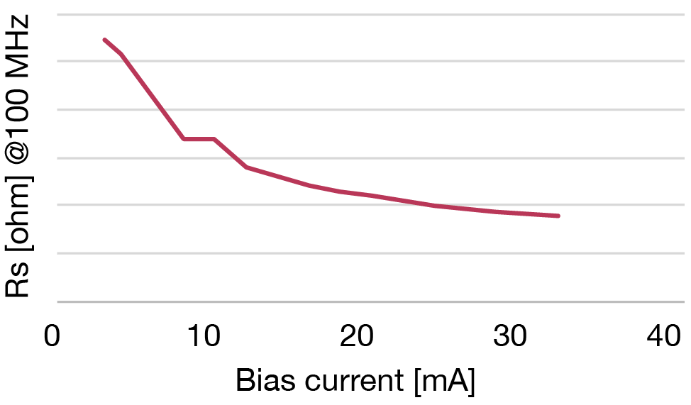
PIN diodes operate as a variable resistor when a forward voltage is applied to cause a forward current to flow. This characteristic, known as high-frequency forward resistance, is often expressed as “Rf” on datasheets. The high-frequency forward resistance Rf is generally measured at 100 MHz while applying a DC current.
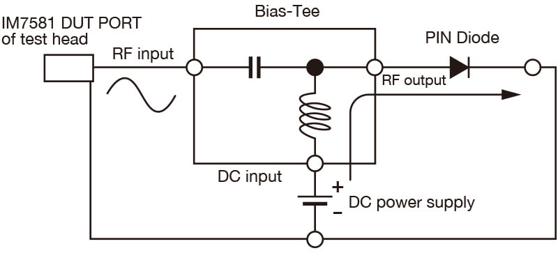
Please see the figure for bias-tee connections. This component blocks DC current from the DC power supply so that it does not flow to the IM7581. In addition, the IM7581’s 100 MHz measurement signal is blocked by a choke coil in the bias tee so that it does not flow to the DC power supply. Use of the bias tee makes it possible to measure high-frequency forward resistance at 100 MHz while feeding a DC current to the PIN diode.
Measurement Data
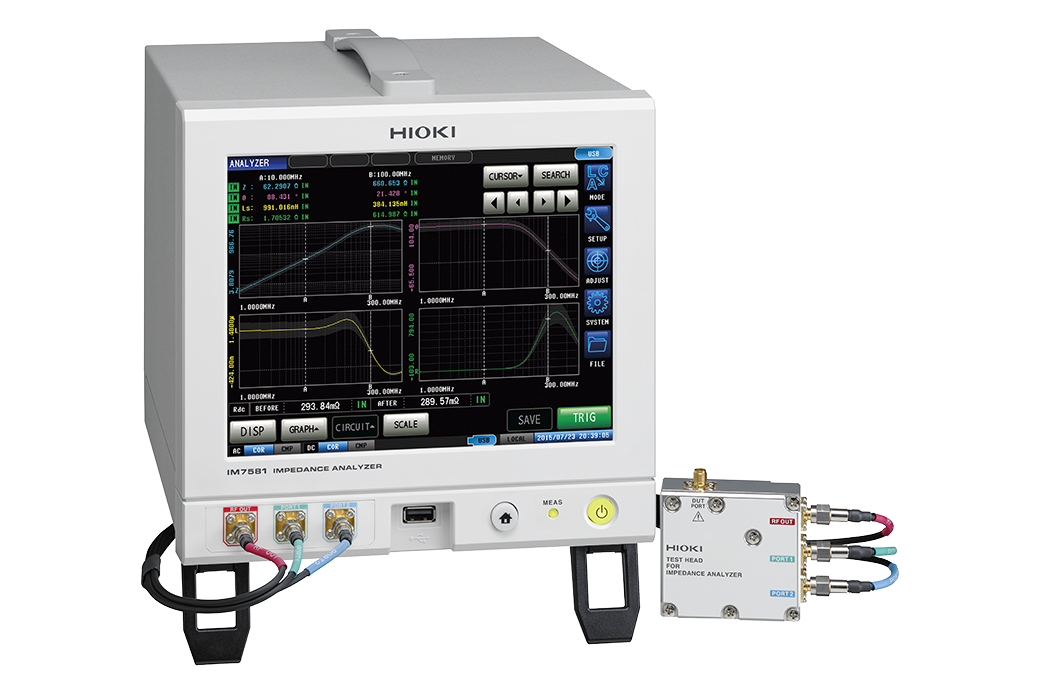
The following data was obtained by measuring a PIN diode with the IMPEDANCE ANALYZER IM7581-01.
Measurement-related precautions and key considerations when choosing a Bias-tee
- Include the Bias-tee and power supply in OS compensation
- Perform compensation while the DC power supply is outputting 0.00 A
- Place the power supply in a 0.00 A output state
- Choose a Bias-tee model that exhibits flat frequency characteristics near the measurement frequency
- Exercise care concerning heating caused by current flowing to the path resistance and contact resistance