Product Jun. 06, 2025
Hioki Begins Accepting Orders for the FA1823 Flying Probe Tester—Enabling Reliable Four-Terminal Testing of Ultra-Fine Pads on Advanced IC Package Substrates
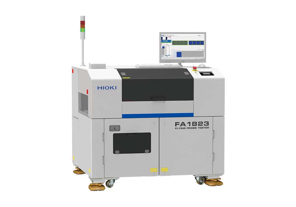
FA1823 Flying Probe Tester Capable of Probing Ultra-Small Pads
Nagano, Japan, 6th June 2025 – Hioki E.E. Corporation has announced the start of order acceptance for the new FA1823 Flying Probe Tester, engineered to meet the demands of ongoing miniaturization in IC package substrates1. Product shipments are scheduled to begin around October 2025.
The FA1823 offers high-precision probing on ultra-fine pads as small as Φ 19 μm, and for the first time in the industry2—enables four-terminal low-resistance (Kelvin) measurements3 on pads of this scale. By addressing key challenges in R&D, quality assurance, and mass production, the FA1823 significantly enhances inspection yield and long-term reliability in IC package substrate manufacturing.
Development Background
Artificial-intelligence technologies are expanding rapidly across the globe. In the semiconductor industry, surging demand for high-performance computing (HPC), electric vehicles (EVs) and 5G connectivity is accelerating the need for greater computing performance and lower energy consumption. To address these evolving needs, IC packaging is shifting towards chiplet architectures and 2.5D/3D integration4, leading to finer design features and higher component density. In cutting-edge packages such as advanced FCBGA5, silicon bridge6, and glass substrate7packages, pad diameters and wiring pitches are shrinking at a rapid pace. As a result, electrical inspection now demands ultra-high contact accuracy and exceptional measurement resolution – capabilities that traditional test systems struggle to deliver.
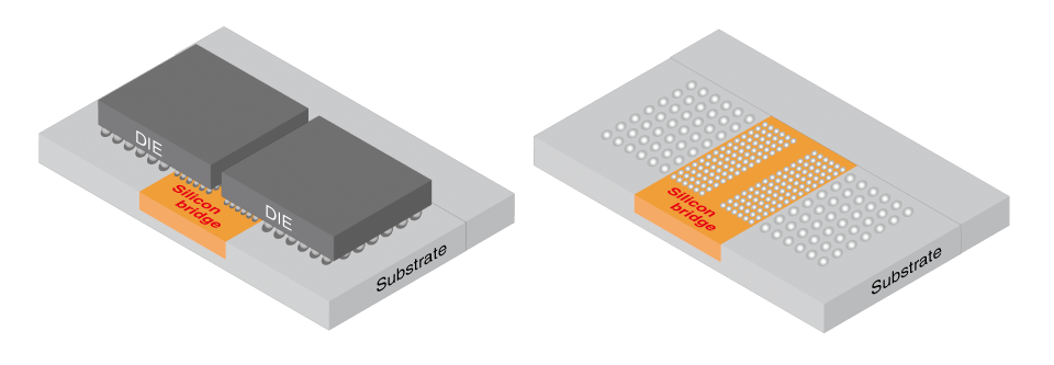
Example of a silicon-bridge substrate
Conventional testers have struggled to keep pace with today’s ultra-fine geometries. Embracing the concept “Probe the Unprobeable.”, Hioki has completely redesigned the FA1823’s mechatronic systems and measurement algorithms, pushing the performance boundaries of flying-probe testers. In addition to standard open/short testing, the FA1823 enables lot-level quality evaluation through precision line-resistance measurements, empowering users to optimize manufacturing processes. By enabling accurate inspection of high-density IC packages, Hioki contributes to the advancement of next-generation technologies that help address a wide range of global and societal challenges.
Key Features
1. High-Precision Probing on Φ 19 μm Pads
A newly engineered high-rigidity frame, automatic probe calibration, and ultra-fine Kelvin probes collectively deliver approximately 67 % improvement in probing accuracy over the previous model. With a positioning resolution of 0.1 μm, the FA1823 enables reliable contact even on the ultra-small pads—laying the groundwork for future support down to Φ 15 μm.
2. Industry-First Four-Terminal Measurements on Ultra-Fine Pads
The FA1823 is the first in the industry to offer four-terminal (Kelvin) measurements on such small pads. This method eliminates errors caused by contact and lead resistance, enabling high-speed, mΩ-level resistance testing. As a result, users can perform lot-quality evaluations based on actual measured values.
3. Streamlined Probe Replacement and Maintenance
Probe replacement is now simpler and more reliable. Fully automated post-replacement calibration eliminates the need for manual adjustments, reducing downtime, minimizing operator workload, and improving consistency by eliminating human error.
Main Applications
- Continuity, insulation, and line-resistance testing of FCBGA IC package substrates
- Electrical testing of substrate for hybrid packages with silicon bridges
- Quality inspection of RDL8 prototypes and development samples for 2.5D/3D chiplets
- Inspection of high-density BGA substrates for AI accelerators9, HPC, GPUs10, and EV ADAS11 power-module applications
Contact us
For inquiries such as quotes, demonstrations, and trial usage, please use Hioki’s contact form for a personalized reply from your closest or most appropriate Hioki representative.
-
Notes:
- 1IC package substrate: A multilayer intermediate board that routes power and signals between a die (semiconductor chip) and the final printed circuit board (PCB). Includes interposers and IC substrates.
- 2According to HIOKI research (as of May 2025): FA1823 is the only flying-probe tester that standard-equips four-terminal low-resistance measurement for Φ 19 μm pads.
- 3Four-terminal low-resistance (Kelvin) measurement: A method that separates current and voltage terminals to eliminate contact and lead resistance, enabling high-accuracy resistance measurements.
- 42.5D/3D IC chiplet: Technology that densely integrates multiple dies in close 3-D proximity to create high-performance, low-power IC packages.
- 5FCBGA (Flip-Chip Ball-Grid Array): A high-density package where the chip is flip-chip mounted and connected via solder balls on the substrate underside, offering superior heat dissipation.
- 6Silicon bridge: A silicon interposer with ultra-fine terminals that interconnects multiple chips at narrow pitches, enabling high-speed signaling while minimizing substrate area.
- 7Glass substrate: An emerging alternative to organic substrates, offering high density mounting, high-frequency performance, and high thermal conductivity for advanced semiconductor packages.
- 8RDL (Redistribution Layer): A wiring layer that reroutes chip pads, achieving higher density, multilayer connections, and miniaturization on IC package substrates.
- 9AI accelerator: A processor specialized for AI computations, executing matrix operations at high speed and low power to accelerate training and inference.
- 10GPU (Graphics Processing Unit): A parallel processor originally for graphics; now in high demand for fast AI inference and training.
- 11ADAS (Advanced Driver Assistance System): Driver-assistance technology that enhances safety using cameras, radar, and other sensors.
- The information provided is current as of the date of publishing.
- Please note that prices, specifications, and other information contained in this texts are subject to change without notice.
- The company names and product names used in this text are registered trademarks or trademarks of their respective companies.
About HIOKI
Established in 1935, HIOKI E.E. CORPORATION (TSE: 6866) has grown to become a world leader in providing consistent delivery of test and measuring instruments through advanced design, manufacturing, and sales and services. By offering over 200 main products characterized by safety and quality while meeting an expansive range of applications, we aim to contribute to the efficiency and value of our customers' work in research and development, production and electrical maintenance. Hioki products and services are available around the world through our extensive network of subsidiaries and distributors. For more information, visit us at www.hioki.com.