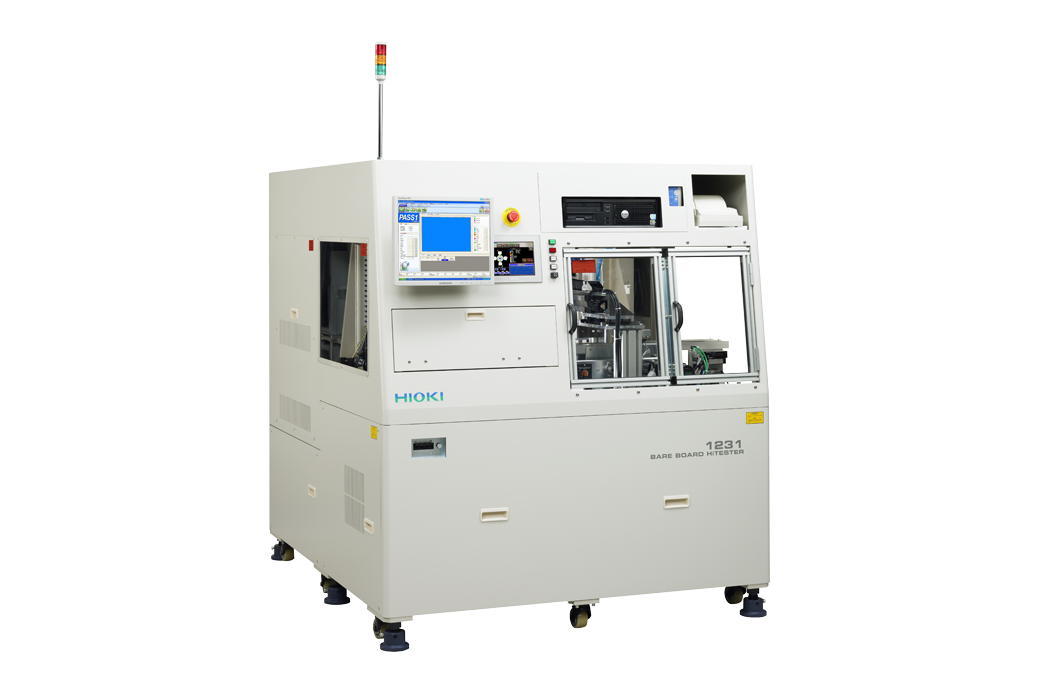
BARE BOARD HiTESTER 1231
Semiconductor Package Board Testing System Utilizing Index Table Method
Discontinued
The 1231 is an IC package board tester that features high-precision, large-pin capabilities for high-density, fine-pitch boards.
- Index table method
Index-type system simultaneously supplies, aligns, tests, and ejects boards, providing wait-free multitasking performance.
- Support for probing fine patterns
High repeatability makes it possible to probe within an area with a diameter of 10 μm.
- Support for high-density wiring boards
The 1231-11 can perform 4-terminal testing of high-density wiring boards with up to 16384 pins (200% more than previous models)
- Intuitive user interface
Easy-to-understand icons facilitate intuitive operation. The 1231-11 also supports graphical display of electronic component connection information.
- Flip-chip solder bump profile testing
The 1231-11 supports combined testing with Zygo-manufactured systems.
Model No. (Order Code)
| 1231-11 | Discontinued |
|---|
Key Features
• Index table method
Index-type system simultaneously supplies, aligns, tests, and ejects boards, providing wait-free multitasking performance
• Support for probing fine patterns
High repeatability makes it possible to probe within an area with a diameter of 10 μm
• Support for high-density wiring boards
The 1231-11 can perform 4-terminal testing of high-density wiring boards with up to 16384 pins (200% more than previous models)
• Intuitive user interface
Easy-to-understand icons facilitate intuitive operation
The 1231-11 also supports graphical display of electronic component connection information
• Flip-chip solder bump profile testing
The 1231-11 supports combined testing with Zygo-manufactured systems
Specifications Overview
| Maximum number of pins | Max. 16,384 (max. 12,288 on top and max. 4,096 on bottom) Standard: 4,096 pins (8 scanner boards each for top and bottom for a total of 4,096 pins) |
|||||
|---|---|---|---|---|---|---|
| Number of test steps | Max. 10,000 | |||||
| Cycle time | 1.5 sec./piece (1,024 points, continuity testing, isolation testing, 2 points per pattern, measuring a PASS board) |
|||||
| Minimum pad diameter | φ 10 μm | |||||
| Probe working area | 610 mm (24.02 in) W × 510 mm (20.08 in) D | |||||
| Clampable/transportable board dimensions | Thickness: 0.3 to 2.5 mm (*Standard specifications: 0.8 to 2.5 mm) Outer dimensions: 13 mm (0.51 in) W × 13 mm (0.51 in) D to 75 mm (2.95 in) W × 75 mm (2.95 in) D (*Standard specifications: Up to 55 mm (2.17 in)) |
|||||
| Inter-probe pitch | Min. 80 μm | |||||
| Power supply | 200 V AC ±10% (3-phase), 50/60 Hz, 6 kVA | |||||
| Dimensions and mass | 1,500 mm (59.06 in) W × 1,680 mm (66.14 in) H × 1,750 mm (68.90 in) D, 2,000 kg (70,546.7 oz) | |||||
-
BARE BOARD HiTESTER 1231
 English