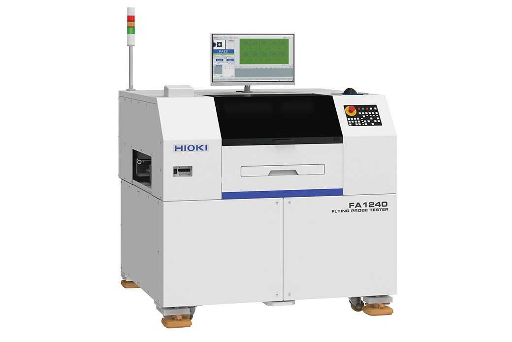
FLYING PROBE TESTER FA1240-6x
Electrical Testing Verifies Correct Mounting
Populated Board Testing System


-
 Compliant: FA1241-61
Hioki PCB and substrate inspection equipment leverages our core competency in high precision component testing. The FA1240 series is a 4-arm populated board inspection tool that delivers multi-functional testing in as fast as 0.025 sec./step.
CE Compliant model: FA1241-61
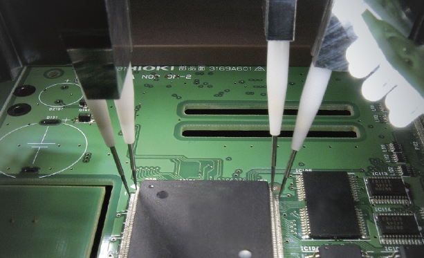
High speed and high accuracy lead-lift inspection
With its unique ultra-thin coaxial probe, it enables rapid lead-lift inspection, including pseudo-contact evaluation.
When combined with the contact-check function, the system achieves highly reliable inspection across all measurement modes.
High speed automatic inspection of terminal welding in battery modules
Using a proprietary ultra-fine probe designed for 4-terminal resistance measurement, the system enables fixture-less, high-speed, high-accuracy inspection of terminal-weld resistance in battery modules. It can reliably access the limited space on the negative side of cylindrical cells to perform 4-terminal measurements.
Key Features
- Quickly complete programs that take into account component height
- Automatically calculate arm interference (when used with the UA1780)
- Designed to improve probe replaceability, dramatically reducing system downtime caused by probe replacement
- High-speed testing at up to 0.025 sec./step
- Proprietary Hioki lead float detection reliably detects issues up to and including pseudo-contact
- Provides a superior level of solder quality assurance
- Phase-isolated measurement and guarding functionality are ideal for analog circuits
- Support for active testing (optional feature)
- Large testing area of 510 × 460 mm (FA1240-61)
- Automatic alignment function and simple visual test function
Model No. (Order Code)
| FA1240-61 | For large boards |
|---|---|
| FA1240-63 | For medium rack boards |
| FA1241-61 | CE compliant model, for large boards |
Electrical Testing Verifies Correct Mounting
Create a program from the design data, perform electrical testing with minimal time and cost, and quickly confirm and record defects.
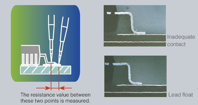
Lead float and pseudo-contact are not the same thing.
Pseudo-contact of leads is a type of defect that may slip through various tests during the board manufacturing process and make its way into the market.
Lead float can be fairly reliably identified by today's image inspection technology.Consequently, Hioki's proprietary resistance measurement pseudo-contact test serves to detect pseudo-contact, which is difficult to identify based on appearance alone.
Focusing on the supreme importance of test points and Gerber data
It's half true, and half untrue, to say that the ability to easily create data is distinct from the ability to easily test boards.Being able to create data easily may have meant being able to test boards easily during the discrete era, but in creating the test data required by the FA1240, it is critical that creating accurate test data be a simple and easy-to-perform process.
By minimizing the difference between data that's good enough to operate the tester and data that's good enough to ship products, it is possible to minimize production line downtime (to allow for debugging and other modifications) and to ship products with peace of mind.
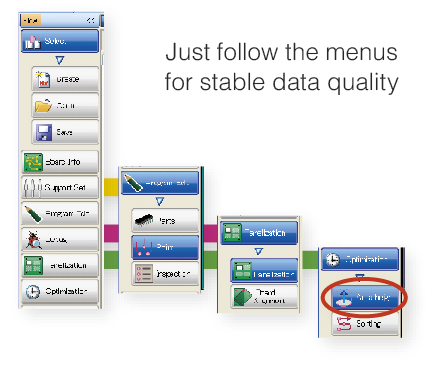
Simply follow the workflow.
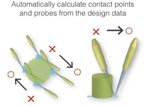
Quickly complete programs that take into account component height
Automatic calculation of arm interference (when used with the UA1780)
Do you check data by looking at probe tips and asking yourself whether they'll strike components on the board or not?
In fact, choosing probes used to be a demanding and time-consuming part of the debugging process that required a high degree of care.By adding component height information to mounting data, the FA1240 is able to automatically select an appropriate test probe, allowing you to approach the task of debugging electrical testing with peace of mind.
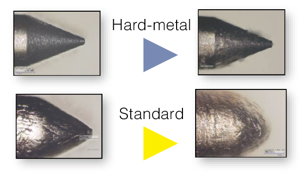
Long-life probes (easy replacement NEW and long service life)
The tips of Hioki's new super-hard probes show no wear, even after 3 million contact cycles.
Stable contact for up to 3,000,000 uses, prevents pseudo-contact due to slips
[Program,Test,Visualize] Populated Board Electrical Testing System
Hioki can prepare populated board testing system benchmarks if provided with the three types of data listed below.
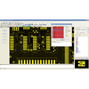
[Program] FIT-LINE UA1780
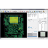
[Test] FLYING PROBE TESTER FA1240
[Visualize] FAIL VISUALIZER UA1782
When testing populated boards, it's essential to create accurate data, measure boards accurately, and identify defective locations accurately.
Specifications Overview
| FA1240-61 FA1241-61 |
FA1240-63 | |||||
| Number of arms | 4 (L, ML, MR, R) | |||||
| Number of test steps | 40,000 (max.) | |||||
| Measurement ranges | Resistance: 400 μΩ to 40 MΩ Capacitance: 1 pF to 400 mF Inductance: 1 μH to 100 H Diode VZ measurement: 0 to 25 V Zener diode VZ measurement: 0 to 25 V, 25 to 80 V (optional feature) Digital transistors: 0 to 25 V Photo couplers: 0 to 25 V Short: 0.4 Ω to 400 kΩ Open: 4 Ω to 40 MΩ DC voltage measurement: 0 to 25 V |
|||||
| Measurement time | Max. 0.025 sec./step | Max. 0.025 sec./step | ||||
| Probing precision | Within ±100 μm for each arm (X and Y directions) | |||||
| Positioning repeatability | Within ±50 μm (probing positions) | |||||
| Inter-probe pitch | Min. 0.15 mm Min. 0.5 mm (when using 4-terminal probes) |
Min. 0.15 mm Min. 0.5 mm (when using 4-terminal probes) |
||||
| Testable board dimensions | 510 mm (20.08 in) W × 460 mm (18.11 in) D | 400 mm (15.75 in) W × 330 mm (12.99 in) D | ||||
| Power supply | 200 V AC (single-phase), 50/60 Hz, 6 kVA (FA1241: 230 V AC) | 200 V AC (single-phase), 50/60 Hz, 5 kVA |
||||
| Dimensions and mass | 1406 mm (55.35 in) H × 1300 mm (51.18 in) H × 1380 mm (54.33 in) D, 1150 kg (40,564.4 oz) | 1266 mm (49.84 in) H × 1369 mm (53.90 in) H × 1425 mm (56.10 in) D, 1050 kg (37,037 oz) | ||||
Options (2)
FIT-LINE INSPECTION DATA CREATION SYSTEM
OFF-LINE SOFTWARE FA1139-09