Product Dec. 12, 2025
Hioki Begins Accepting Orders for the FA1815-01/-11 Flying Probe Tester—High-Speed, High-Precision Technology for Diverse Substrate Inspections
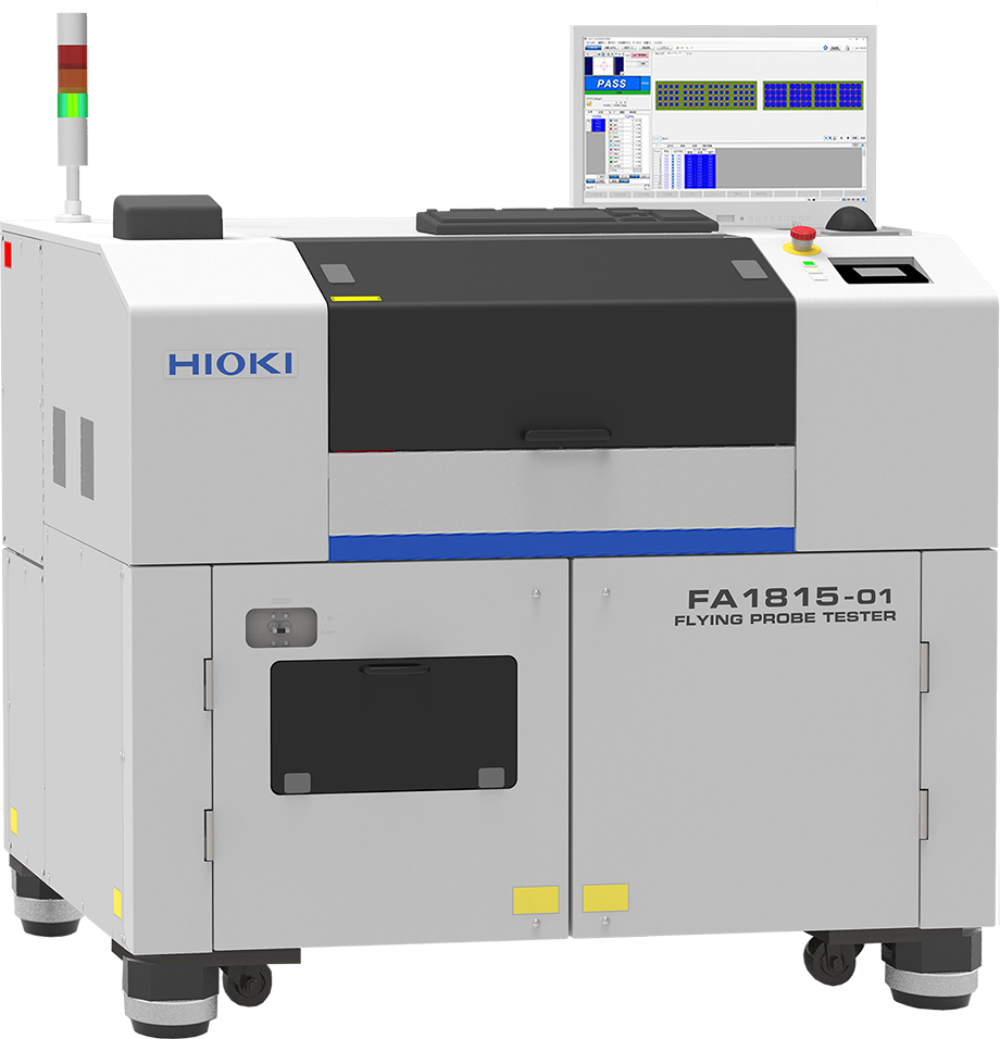 Flying Probe Tester FA1815-01
Nagano, Japan, 12th December 2025 – Hioki E.E. Corporation is pleased to announce that orders are now open for the new FA1815-01/-11 Flying Probe Tester, supporting a wide range of substrates—from high density multi-layer boards and ceramic boards to high-density IC substrates*1. The product is scheduled to be released in April 2026. The FA1815-01/-11 delivers faster and more precise probing than previous models, integrating proprietary technologies that enhance speed, accuracy, and cost efficiency. Designed to address key challenges faced in development, quality assurance as well as manufacturing environments, the new system significantly improves inspection yield rate and long-term reliability on production lines.
Background of Development
With trend of electronic devices development, IC substrates are rapidly increasing in density. Conventional jig-based testers are reaching their limits, struggling both technically and economically to keep up with the inspection needs of high-density substrates. While flying probe testers have emerged as an alternative, traditional models often force users to choose between speed and accuracy. High-speed, multi-head systems with high precision were also priced at a premium, causing barriers to adoption.
In response to these market challenges, Hioki has newly developed a flying probe tester that optimizes both probing accuracy and inspection speed while keeping accessible and cost-effective. The new FA1815 series supports diverse inspection requirements and helps manufacturers enhance efficiency and reduce operating costs.
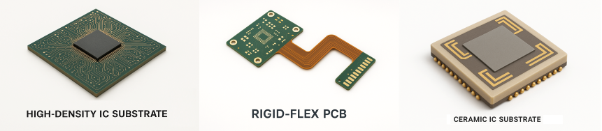 Supports a wide variety of substrates
Product Features
1. High-speed inspection up to 100 Points/Second with Enhanced Probing Accuracy
Maintaining high probing accuracy during high-speed movement requires minimizing mechanical vibration and environmental interference. The FA1815 series achieves this through a newly engineered rigid frame and up-to-date motor control technology that minimize vibration and external influences, enabling highly precise probing—even at maximum inspection speeds.
2. DUT-friendly 10V/100GΩ low-voltage insulation resistance testing
High-voltage insulation resistance testing is effective for detecting latent defects that can lead to malfunctions or failures but carries the risk of damaging delicate circuit trace. Leveraging Hioki’s micro-current measurement technology, the FA1815 series enables insulation resistance testing up to 100 GΩ at only 10 V, achieving reliable inspection results while significantly reducing the risk of substrate damage.
3. Value-added Capacitance and Embedded Component Measurement for Versatile Board Inspection
The system supports capacitance measurement and inspection of embedded components such as diodes. Combined with in-circuit-tester-based embedded component inspection technology, Hioki's high-speed capacitance measurement method accommodates a wide range of applications. Based on decades of expertise in precision measurement, Hioki offers precise and reliable measurement solutions.
Main applications
- Continuity, insulation, and wiring resistance testing of FCBGA*2 type IC substrates
- Electrical testing of hybrid substrate with silicon bridge*3
- Quality inspection of RDL*4 prototypes and developed products for 2.5D/3D IC chiplet*5
- Inspection of high-density substrates for 5G and IoT semiconductor devices
- Inspection of substrates for high-performance products such as smartphones, wearables, and autonomous vehicles
Product Lineup
- Flying Probe Tester FA1815-01: Horizontal, double-sided, off-line type
- Flying Probe Tester FA1815-11: Horizontal, double-sided, in-line type
Order Start Date
December 12, 2025
Product Release Date
April 30, 2026
Notes
- *1:IC substrate: A multilayer intermediate substrate used between the semiconductor die and the PCB to route electrical signals and power. Includes interposers and IC substrates.
- *2:FCBGA (Flip Chip Ball Grid Array): A high-density package format in which chips are flip-chip mounted and connected via solder balls, offering excellent heat release.
- *3:Silicon bridge: A silicon interposer with ultra-fine terminals enabling multi-chip connections in narrow pitches, improving signal speed while reducing substrate area.
- *4:RDL (Redistribution Layer): A wiring layer that rewires chips on IC substrates to achieve higher density, multilayer interconnections as well as miniaturization.
- *5:2.5D/3D IC chiplet: Technology enabling compact, high-density, high-speed, low-power IC substrates by arranging and interconnecting dies in close proximity within a stacked or semi-stacked configuration.
Contact Us
For quotations, demonstrations, or trial run requests, please reach out through Hioki’s contact form. A representative from your nearest Hioki office will respond to you directly.
- The information provided is current as of the date of publishing.
- Please note that prices, specifications, and other information contained in this texts are subject to change without notice.
- The company names and product names used in this text are registered trademarks or trademarks of their respective companies.
About HIOKI
Established in 1935, HIOKI E.E. CORPORATION (TSE: 6866) has grown to become a world leader in providing consistent delivery of test and measuring instruments through advanced design, manufacturing, and sales and services. By offering over 200 main products characterized by safety and quality while meeting an expansive range of applications, we aim to contribute to the efficiency and value of our customers' work in research and development, production and electrical maintenance. Hioki products and services are available around the world through our extensive network of subsidiaries and distributors. For more information, visit us at www.hioki.com.